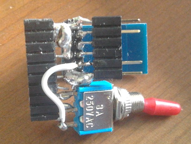
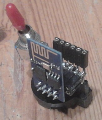
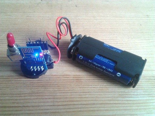
Connector layout for ESP8266-01
Hi,
I had problems in flashing ESP8266-01 from Arduino IDE and got help on Github:
https://github.com/esp8266/Arduino/issu ... -106367956
I knew that CH_PD and VCC had to be connected to VC of USB2TTL before, and learned there that RESET has to be connected to VC as well.
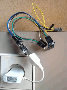
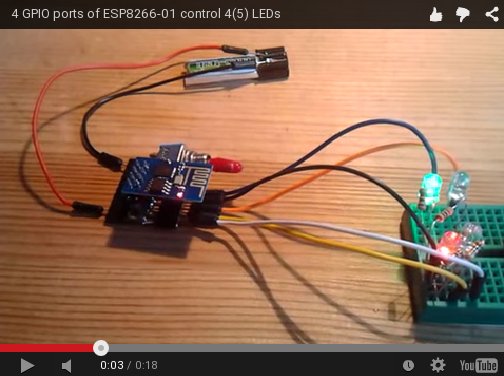
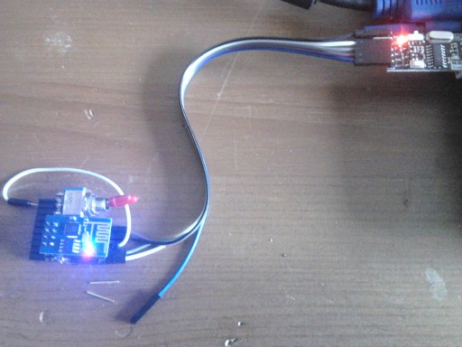
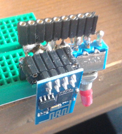
Based on that knowledge I soldered a stand for ESP8266-01 that has bottom 9 female pins for connecting coin cell connector, horizontal 2x6 female (for connecting ESP8266-01 in the middle 2x4 and top 6pin female providing all 6 variable connections [TXD/GND/GPIO2/GPIO0/RXD/VCC(=RST=CH_PD)].
After I learned that coin cells cannot provide the current needed by ESP8266-01 I added another connector fitting into the bottom 9pin connector and being plugged directly into 3.7V LiPO. With that I got nice "Standalone small outdoor #Wifi #access #point and #webserver":
https://twitter.com/HermannSW/status/604621715554091008
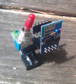
My question now is whether the 6pin 1line connector layout at top is good?
Seems to provide everything needed (even setting GPIO0 to GND for flashing).
Hermann.
I had problems in flashing ESP8266-01 from Arduino IDE and got help on Github:
https://github.com/esp8266/Arduino/issu ... -106367956
I knew that CH_PD and VCC had to be connected to VC of USB2TTL before, and learned there that RESET has to be connected to VC as well.
Based on that knowledge I soldered a stand for ESP8266-01 that has bottom 9 female pins for connecting coin cell connector, horizontal 2x6 female (for connecting ESP8266-01 in the middle 2x4 and top 6pin female providing all 6 variable connections [TXD/GND/GPIO2/GPIO0/RXD/VCC(=RST=CH_PD)].
After I learned that coin cells cannot provide the current needed by ESP8266-01 I added another connector fitting into the bottom 9pin connector and being plugged directly into 3.7V LiPO. With that I got nice "Standalone small outdoor #Wifi #access #point and #webserver":
https://twitter.com/HermannSW/status/604621715554091008

My question now is whether the 6pin 1line connector layout at top is good?
Seems to provide everything needed (even setting GPIO0 to GND for flashing).
Hermann.
