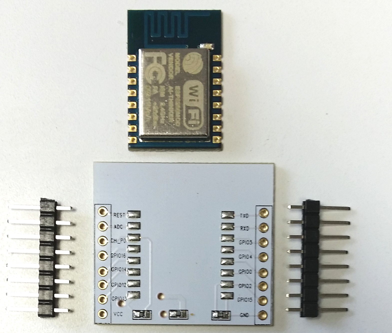
Anyone knows what are the exact schematics for this board? i googled 20 minutes could not find it
Board is similar to this:

Explore... Chat... Share...

martinayotte wrote:The schematic can be deducts easily just by looking at the trace in the above picture.
The left resistor is 10K pullup on CH_PD and the right resistor is 10K pulldown on GPIO2.
The middle resistor is probably a 0 ohms for optional 3V regulator that can be added at the back of the PCB.
Barnabybear wrote:but I'm guessing there is something on the back that is impotant as you wouldn't expect a pull down on GPIO 2. Both GPIO 0 & GPIO 2 should be pulled up (10k ish) for normal operation.
It takes about 20-25 seconds for home assistant c[…]
I tried to upgrade tof my sonoff basic R2 with the[…]
a problem Perhaps you want to define "Probl[…]
Rebooting your router will not give you a faster I[…]
There are no other notifications from esptool.py i[…]
Using the Arduino IDE, you'll learn how to set up […]
In this project, you will post to Twitter using an[…]
In this project, we will build a water level contr[…]
I guess I'm late, but I had the same problem and f[…]
Last night I received my first D1 Minis for a lear[…]
Although I am aware that this is an old post, I fe[…]